 Why HARTING component carriers are now replacing flexible PCBs: Part 1
July 30, 2020 REDWIRE is news you can use from leading suppliers. Powered by FRASERS.
Posted by Harting Canada Inc
The family-owned HARTING Group is a global leader in connectivity solutions. HARTING invented the modular connector and... Read more
Subscribe
Free REDWIRE e-newsletter
HARTING has developed a new solution that replaces flexible circuit boards.
In this two-part article, HARTING Canada discusses the considerable advantages that component carriers have over flexible printed circuit boards (PCBs).
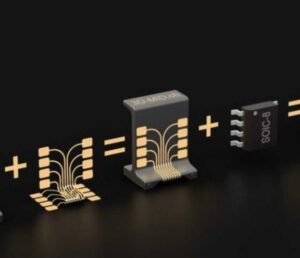
Flexible circuit boards offer numerous advantages. However, the mechanical fixation of these circuit boards is highly complex. HARTING has developed a new solution based on 3D-MID (moulded interconnect device) technology that replaces flexible circuit boards. Thanks to component carriers, some customers are seeing significant cost savings.
Flexible PCBs are made of thin polyimide films and have been used for many years in a wide array of applications. Populating and assembling them, however, is complex, which has led device manufacturers to demand a better solution. This is where a newly developed component carrier from HARTING enters the picture.
A standardized component carrier for electronic components
By harnessing this new HARTING development, electronic components can be placed directly onto the component carrier, replacing flexible circuit boards. The component carrier serves as a connecting element between the printed circuit board (PCB) and electronic components such as LEDs, ICs, photodiodes, and sensors.
The populated component carriers are delivered in tape and reel. In their standard design, the carriers can be processed in automatic assembly systems, just like other SMD electronic components. Two different sizes are currently available and can accommodate electronic components of standard size SOIC-8 and smaller. Moreover, HARTING can produce the carriers in customer-specific sizes.
HARTING has identified three example applications where the component carrier can replace flexible circuit boards:
- Components at a 90-degree angle to the circuit board: The component carrier is suitable for scenarios in which electrical components, such as sensors, need to be positioned at a 90-degree angle to the circuit board. The automatic assembly process enables the placement of temperature sensors or hall sensors on the carrier to a high degree of accuracy, which results in precise, reproducible measurements. Another salient example is optical components, such as LEDs or photodiodes used to generate precise light barriers.
- Clearance from the circuit board: The component carrier also makes it possible to maintain a clearance between the circuit board and an electronic component. Consequently, a temperature sensor can be used to measure the temperature in the housing without being influenced by the excess heat from other components on the PCB. It also means that an LED can be placed clear of the circuit board, thereby avoiding the risk of surrounding components casting shadows.
- Antenna function: The component carrier can be manufactured using different base polymers. In this way, different antenna material properties can be factored in, such as dielectric constant and loss factor. The specific antenna layout can be used for various applications in the MHz and GHz frequency range, such as Bluetooth, WiFi, Zigbee, and 5G.
3D-MID technology as an alternative to flexible PCBs
Thanks to the 3D-MID technology, electronic components can be placed directly onto a three-dimensional body without the need for circuit boards or connecting cables. The base body is produced through injection molding, whereby the thermoplastic is provided with a non-conductive, inorganic additive. In order for this material to accommodate electrical circuits, the additives in the plastic are “activated” through laser direct structuring (LDS). In this process, the laser beam writes the areas intended for the conductive tracks and creates a micro-rough structure. The metal particles released in the process form the nucleus for the subsequent chemical metallization.
Coming in Part 2: The advantages of the new 3D-MID component carrier
To learn more, contact HARTING.
Share
Posted by Harting Canada Inc
The family-owned HARTING Group is a global leader in connectivity solutions. HARTING invented the modular connector and... Read more